- Flex PCB Blog
- PCB Assembly Blog
- FPC Research Blog
- Preparation of FPC based on ultrasonic spraying method_4_Experimental Results
- Preparation of FPC based on ultrasonic spraying method_3_Experimental Procedure
- Preparation of FPC based on ultrasonic spraying method_2_Experimental Platform and Principle
- Preparation of FPC based on ultrasonic spraying method_1_abstract
- Research on Layout Design Method of Ultra-thin FPC_4_Analysis of Layout Design Methods
- Research on Layout Design Method of Ultra-thin FPC_3_Analysis of Layout Design Methods
- Research on Layout Design Method of Ultra-thin FPC_2_Analysis of Layout Design Methods
- Research on Layout Design Method of Ultra-thin FPC_1_introduction
- Research progress on polyimide FPC_2_the field of FPC
- Research progress on polyimide FPC_1_Introduction
- Analysis of Vibration Characteristics of FPCBs _4_Summary
- Analysis of Vibration Characteristics of FPCBs _3_Finite Element Analysis
- Analysis of Vibration Characteristics of FPCBs _2_Theory of Vibration Analysis
- Analysis of Vibration Characteristics of FPCBs Under Random Vibration_1_Introduction
- Design Methods for FPCBs_5_Practical Application
- Design Methods for FPCBs_4_Electrical Circuit Design and Examples
- Design Methods for FPCBs_3_Structure Design Method and Examples
- Design Methods for FPCBs_2_Component Selection Methodology and Examples.
- Research on Design Methods for FPCBs
- Application of MPW technique for FPCBs _4_Summary
- Application of MPW technique for FPCBs_3_Experimental results
- Application of MPW technique for FPCBs_2_Experimental setup
- Application of MPW technique for FPCBs_1_Principle of MPW
- Application of FPCB in PC motherboards_4_ Results and discussion
- Application of FPCB in PC motherboards_3_ Numerical analysis
- Application of FPCB in PC_2_ Experimentation
- Application of FPCB in PC motherboards
- A Bus Planning Algorithm for FPC Design _4_Experimental result
- A Bus Planning Algorithm for FPC Design _3_Proposed Algorithm
- A Bus Planning Algorithm for FPC Design _2_Preliminaries
- A Bus Planning Algorithm for FPC Design _1_Introduction
Application of magnetic pulse welding technique
for flexible printed circuit boards (FPCB) lap joints_3_ Experimental results and discussion
4. Experimental results and discussion
4.1. Current signal and collision speed
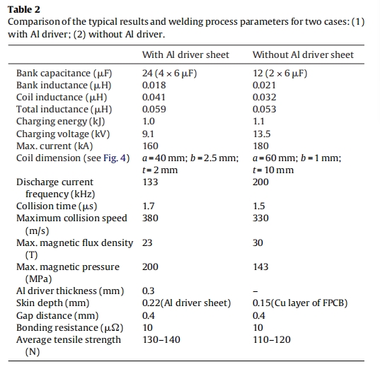
All three different capacitor banks system (CB1, CB2 and CB3) was tested to get the optimum results. The best results were obtained with CB2 system. The minimum joule heating effect and also smallest deformation on FPCB sheets was observed by CB2 system which had a lower total inductance and faster discharge. Typical current waveform (top signal) and also the signal of collision speed circuit (bottom signal) for CB2 system are shown in Fig. 6.This current signal was obtained at 1.0 kJ discharge by using a magnetic probe. The current signal shows that a damping and oscillating current flows through a one-turn coil for the duration of about 50 μs and the discharge frequency was about 133 kHz. The maximum current and maximum magnetic flux density were measured about 160 kA and 23 T at 1.0 kJ discharge in case of using Al driver sheet. The maximum magnetic pressures were calculated by Eq. (2) and it was about 200 MPa for the same discharge.
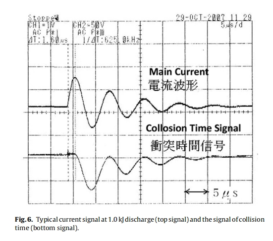
In order to measure the time of collision and also the collision speed of the aluminum driver sheet just before welding,very simple circuit is prepared to measure the time traveling of the base metal in gap distance which is exist between two FPCB sheets before weld- ing. The detail of this circuit is reported in pervious work (Aizawa et al.,2007). The time between starting discharge and final phase of welding was approximately about 1.7 μs and the maximum collision speed of Al driver sheet just before welding is calculated to be 380 m/s.
4.2. Effect of gap between FPCB sheets before welding
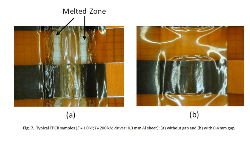
The collision speed has a relation with the bank energy and the discharge current and the maximum collision speed can be obtained at the first maximum in the current signal. Therefore, by inserting the appropriate gap distance between sample sheets, the collision time can be nearly same as quarter period of the current signal at the first maximum current peak. The optimum gap distance has relation with the capacitor bank energy and the discharge system inductance. However, our experimental result shows that 0.4 mm, gap distance between FPCB sheets is necessary for achieving high weld quality. On other hand, the surfaces of FPCB sheet can be melted because of high Eddy current and increasing of Joule heating effect in case of samples without inserting gap between them (Fig. 7).
4.3. Microstructure of joined interface
Fig. 8 shows the lap-joints of three types of FPCB sheets. The width of the weld zone was nearly equal to the middle part of the coil (b =2.5 mm). The welded area has concentrated into two lines with 0.6 mm wideness along of middle part of coil and no heat affected area was observed in polyimide substrate. The lap-joints of W5-FPCB and W10-FPCB sheets divided to several parts for the optical microscope observations and also for shearing strength test.The divided test parts were polished for observing the joined interface. Fig. 9 shows the optical microscope images of the welded area. These optical images show the welded zone was formed in two parts with approximately 2 mm apart. The pictures show a wavy transition layer without any significant heat-affected zone or any crack on copper layer is formed in welded zone. The scanning ion microscopic (SIM) image of welding interface also shows a fine-grain microstructure at interface layer.
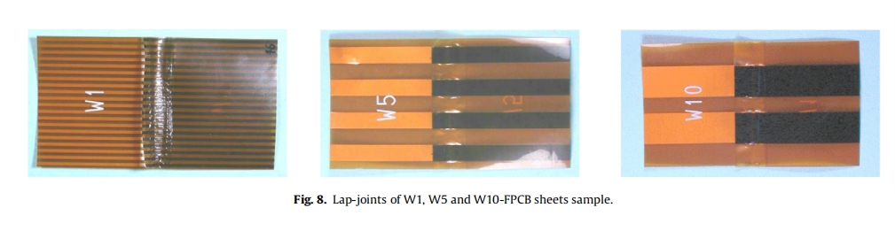
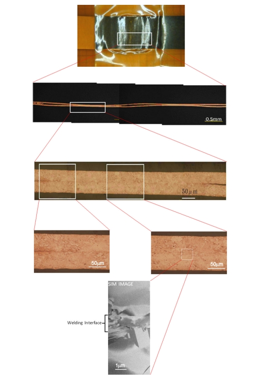
Fig.9. Optical microscope and SIM image of the welded area in FPCB lap-joint.
4.4. Electrical resistances of lap-joints
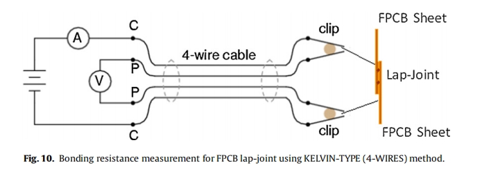
The electrical resistance of FPCB lap-joint was measured by a digital micro-ohmmeter using KELVIN-TYPE (4-WIRES) method.The measurement setup was shown in Fig. 10.It is necessary to remove polyimide films and adhesive materials from welded sample before resistance measurement. The micro-ohmmeter probes should be connected near lap-joint on copper sheet. The bonding resistance of FPCB lap-joints was measured less than 10 μΩ for W5 samples and this value is enough low for micro electronic applications.
4.5. Tensile shear test
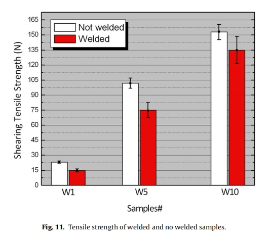
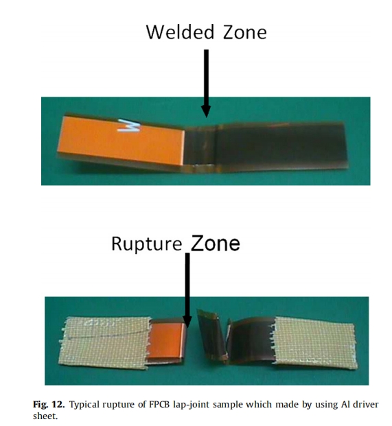
Welded samples were investigated on a standard tensile shear testing machine at test rate of 10 mm/min. The tensile shearing strength of each welded samples (W1, W5 and W10) were measured and compared with results of no-welded samples (Fig. 11). Based on the shearing strength test results, it can be obtained that the maximum tensile shearing of welded sample is little smaller than tensile shearing strength of no-welded FPCB sheet.The maximum tensile shearing for most welded samples was nearly same as tensile shearing strength of copper layer of FPCB sheet and failure always occurred near of welded line (Fig. 12).
4.6. Comparison of results for two cases
The feasibility of MPW technique without using Aluminum driver sheet was investigated and compared with result of Al driver case. In this case, the skin depth is higher than the thickness of the copper layer in FPCB sheet and it is necessary to adjust the appropriate current discharge frequency and increase the total bank energy for obtaining enough high magnetic pressure comparing with using Al driver case. However, the maximum current should be limited to prevent from melting of thin copper layer of FPCB sheet. Several modifications should be considered for reliable welding without using Al driver sheet. The width of middle part of coil was modified to 1 mm to improve eddy current paths and concentration of the magnetic pressure in small area of copper layer. The thickness of coil also was increased to 10 mm for improving the lifetime of coil against mechanical shock of discharge pulse. The maximum dis- charge current and the maximum of magnetic flux density at 1.1 kJ discharge were measured about 180 kA and 30 T, respectively. The maximum magnetic pressures were calculated about 143 MPa for the same discharge. The maximum tensile shearing was obtained about 110–120 N for successful welded samples which is a little smaller than Al driver case. The wavy transition pattern was not so clear in optical microscope observations in this case. For a better comparison of results in both cases, the other typical results and welding process parameters are summarized in Table 2.